Sincerely yours is back from travels to his European lair, Delft where he went to talk about analog integrated circuits, diagnostics, design, and as the Dutch say “koetjes en kalfjes” (a very cute way to say, small talk).
In the meanwhile, the AI chip company Cerebras pronounced its dinner-plate multi-core chips a success, went public and while I respect a bit the hardware nature of the business, cannot but recollect Vespasian’s words “Pecunia non olet” (money does not stink) when he imposed tax on urine. Of course, since the IPO, the stocks of the AI chip company in question started falling and somehow I have the feeling this is only the beginning. If I was of the Las Vegas inclination, I would short the AI.
El Reg reported that Gemini was successfully used in a complicated scheme to steal crypto currency and it is of a minor curiosity that the crook prompted the engine in Russian while the responses were in English. Automation at its best.
In another Orwellian move, Zuckerberg blabbered about feeding his employees keystrokes to the ever data-hungry chat bots.
A latter publicity stunt of AI seems to be going belly-up as the AI agent ordered eggs for an AI-managed coffee shop that has no stove. A Raw egg in your cappuccino, anybody?
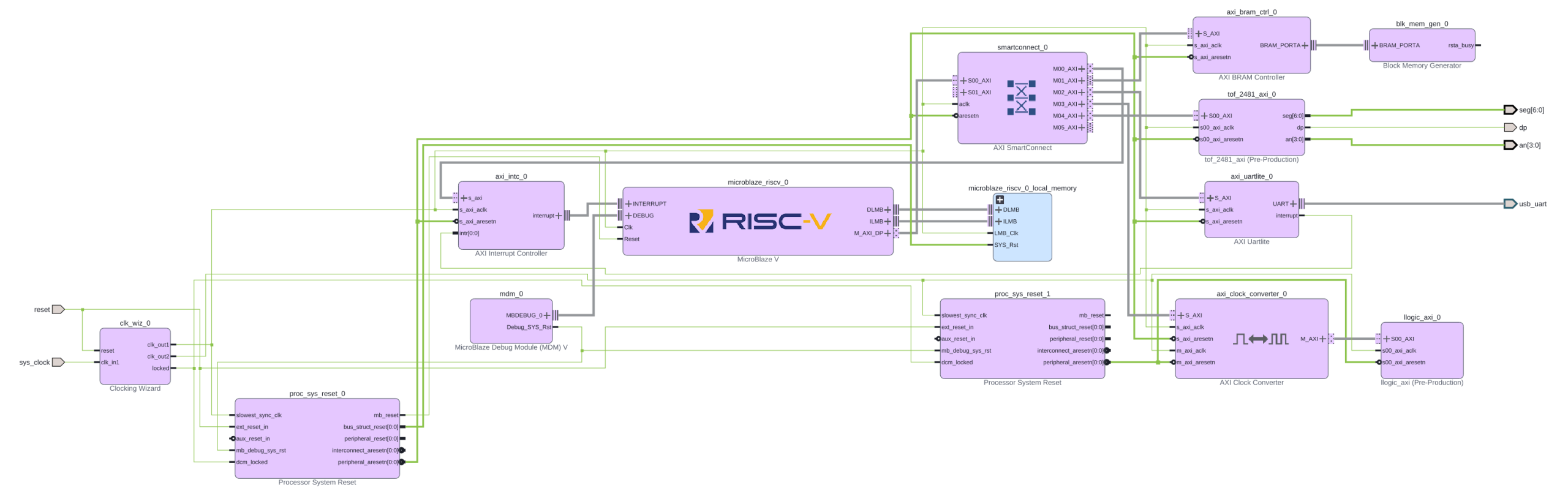
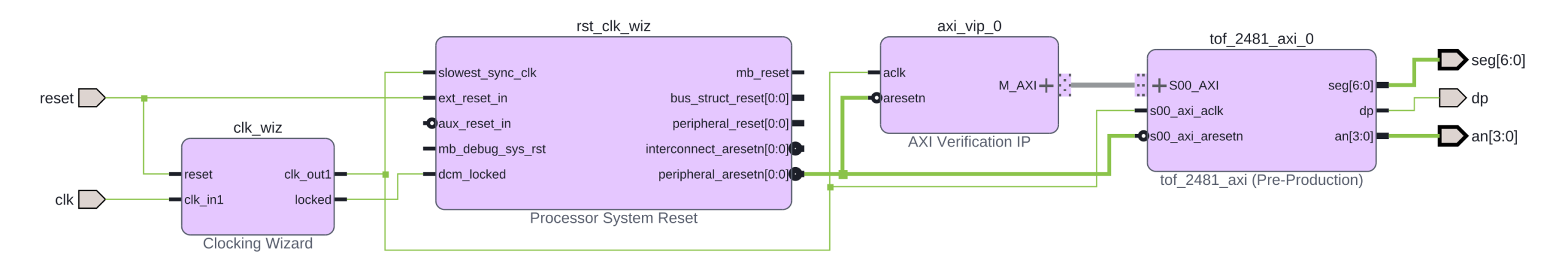
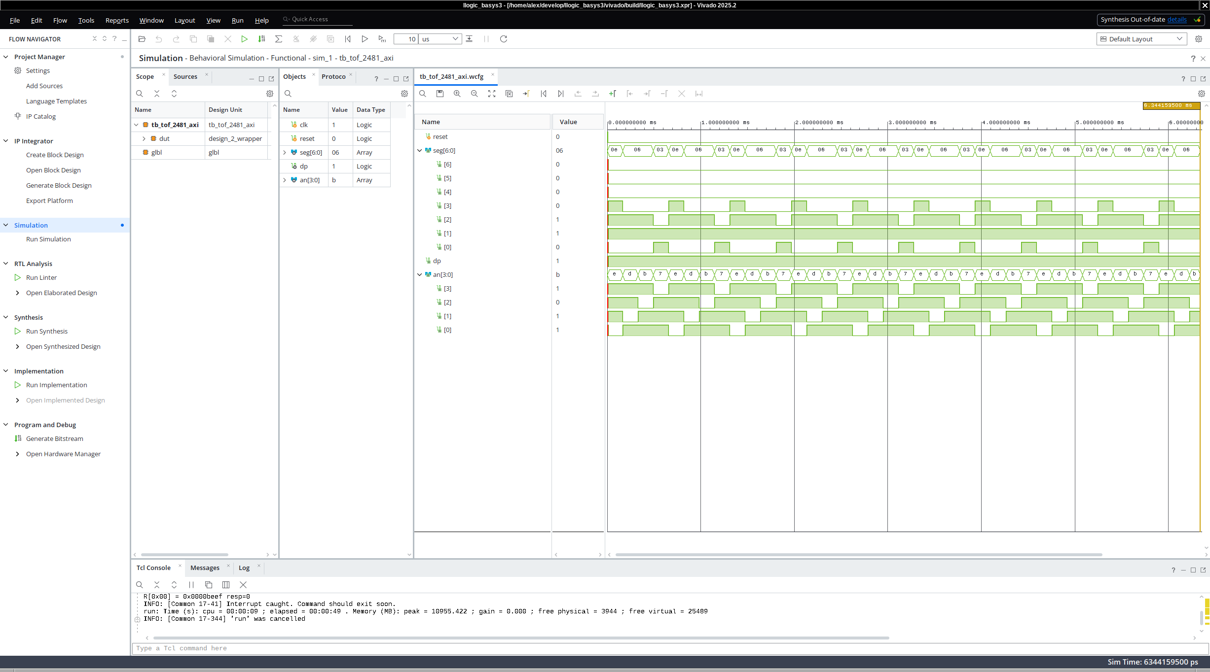
On a less Friday-note I managed to extract an assurance from my TU Delft non-sycophantic human friends that a technology I am working on to provide better Verilog/VHDL technology mapping is not a total hallucination and has fleeting chances of success. More about this in an upcoming blog.
I also went to Delft and talked with a friend about Model-Based Diagnostics, something that used be an AI discipline before the chat-bots vulgarized the term AI. This friend knew about Lydia and the difficulty of modeling the real-world as a system of Boolean equations or a switching circuit. The same friend, didn’t know that after I finished my Ph.D. I spent quite some time figuring the analog alternative of Lydia and extending it.
As I wrote before, Lydia was a system for diagnosis of switching circuits. The process, was somewhat related to model checking. My task was to deal with the computational complexity, which, surprisingly, although very bad in the worst-case was never too bad in practice. Meaning, it was very difficult to come-up with a system that is difficult to diagnose.
The real-problem was, that switching circuits are mostly useful for modeling and designing digital circuits, state-machines, Von Neumann machines and in generals parts of computers. Switching circuits are no good for almost anything physics. This is related to the old debate of causation versus correlation, or the fact that there is no logical implication in physical systems. In other words, in physics and biology, almost everything is some kind of a circuit, almost always with feedback.
Lydia-NG is trying address the difficulty of modeling of physical systems. Of course, I had to provide compatibility with the old Lydia, so I was trying to define diagnosis as multiple simulations, with somewhat random configurations. The configurations that led to simulation predictions close to the actual measurements, would form the diagnostic hypotheses.
I managed to compile and run Lydia-NG and I am in the process of modernizing it. In addition to Boolean systems, Lydia-NG is capable of diagnosing and simulating systems of Ordinary Differential Equations (ODEs), and SPICE models of electrical circuits. SPICE models of electrical systems are somewhat more difficult systems of systems of Differential Algebraic Equations but about that I will talk another time.
Lydia-NG is implemented in C++ and also has an IDE. Below is a simulation of the “Hello, world!” of diagnosis of a chemical system consisting of three connected vessels. You can see what happens whenever there is a leak.
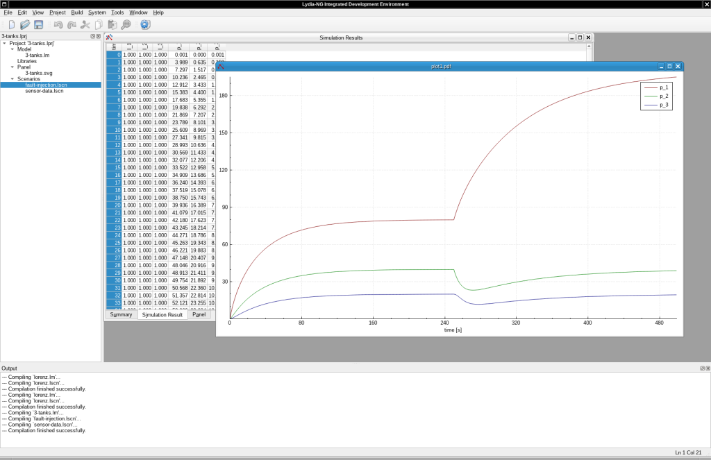
I am in the process of modernizing and finishing Lydia-NG and it and I am thinking on how to release it–open source or otherwise. There is a whole lot to be said about diagnosis of equations and simulation of DAEs, there are also languages like Modelica and communities dedicated to the topic.
There is more to come when talking to state estimation, diagnosis, simulation, and continuous systems. I have implemented techniques like Kalman filters, variations of the latter like Extended and Unscented Kalman Filters (EKF and UKF), particle filters, and many others. Actually, at some point Xerox PARC was trying to prototype a system for diagnosis where tools such as Kalman filters were the core reasoning engine of diagnostics. But about this story, I will write another time.
In another non-development, my application for the South Park Commons, a place for kibitzers to raise money from the naive tech angel investors by talking nonsense, was denied. One can only think of Groucho Marx’s famous quote: “I refuse to join any club that would have me as a member.“