Field-Programmable Gate Arrays and the languages for programming (ahem, configuring them) have the reputation of being difficult to master. I still remember when I heard for the first time: at the beginning of my Ph.D. studies at TU Delft, a new friend of mine, visiting the computer engineering department, came home and told me he was supposed to implement some kind of GPS signal processing that required a lot of linear algebra operations with vectors and matrices (duh, isn’t all computing, including the insanely large vector matrix multiplication of LLMs, like that).
What stroke me at the time is that my friend thought he could just automatically translate Matlab code to VHDL (this is the European version of Verilog, for you Yankees) and benefit from the “micro-parallelism” of the platform. During this phase of my studies, I was already told that turning a sequential algorithm and making it parallel cannot be done by a machine.
But I am diverging. Years later, I still have problems with saying that we program FPGAs. Verilog, VHDL, and SystemC are not classical programming languages like C++ and Python. They have both declarative features for synthesis and procedural features for simulation and fancier techniques like model checking (here I come with my novel ideas and techniques). For the actual physical manifestation of an FPGA like transforming input electrical signals to output signals, the term “FPGA configuration” is more apt than programming. But a job ad for FPGA configurator would sound strange, thus FPGA programming it is!
Demo
Let us fast-forward to the demo. I have felt numerous times the gusto of blinking a LED, so what could be better compared to a bunch of them. In the video below, you can see in action the auto-generated Verilog from the previous article combined with driving the 7-segment LED of the Basys-3.
Of course, this has been done sufficient times and is at the level of a high-school student, if it were not for the connection to the AXI bus, the behavioral simulation and the composition of IP blocks.
Composability and an AXI Architecture for Synthesis
In my previous article on the topic of FPGA, I showed that not all Verilog should be manually written. To do that, I went to implement common digital circuits in Python, saving them as DSLs and translating to Verilog. Of course, testing these circuits with real FPGA hardware requires a lot of infrastructure, and I used Vivado soft processor to do that. Vivado provides a quick graphical way to connect various IP blocks.
I will make a small deviation here. Although these days the boundaries between hardware and software are fuzzy, there is far less open-source hardware than open-source software. The reasons are, I believe, two: first, shipping hardware costs, on top of your time, also cash. The second reason, I believe, is more psychological: that developing hardware provides less instantenous gratification than developing software. That is why the building blocks of electronic chip design are called IP blocks where IP stands for Intellectual Property. Anyhow. Because companies still want to provide closed-source, obfuscated IP blocks, Vivado provides methods for composing these blocks into architectures. And if you want to be anybody in the chip making business you have to adhere to these practices.
One should always be suspicious of acronyms that have both the words Advanced and eXtnsible in them (the I in AXI stands for Interface). But this one is good. It is a part of AMBA and is a standard for chips to connect fast with each other. This is not unlike SPI or I2C, only faster and with many wires.
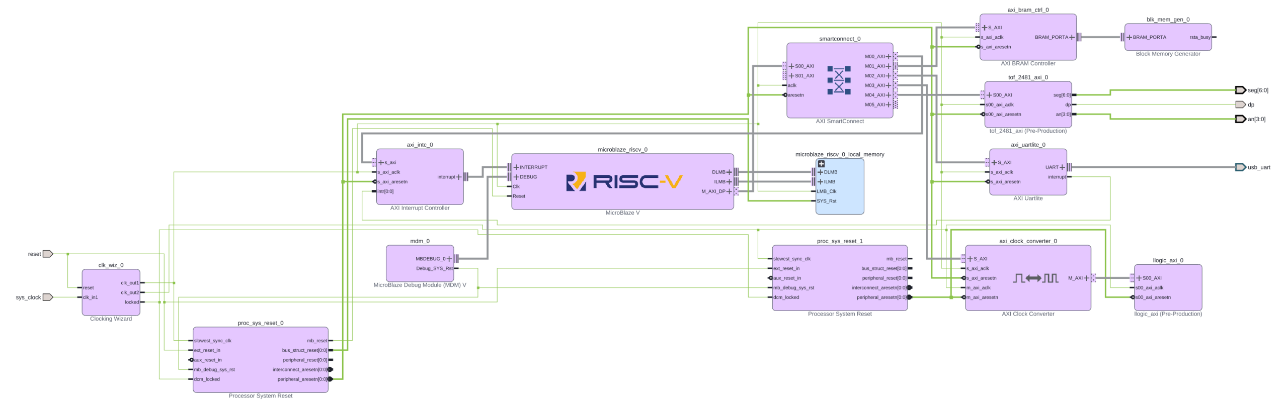
In the previous blog, I showed you the IP block diagram for the RISC-V architecture that uses autogenerated logic circuits. For the demo that follows, I have developed another IP block that drives the 7 segment LEDs of the Basys 3 development board. The new IP block diagram that includes this LED control block is shown below.
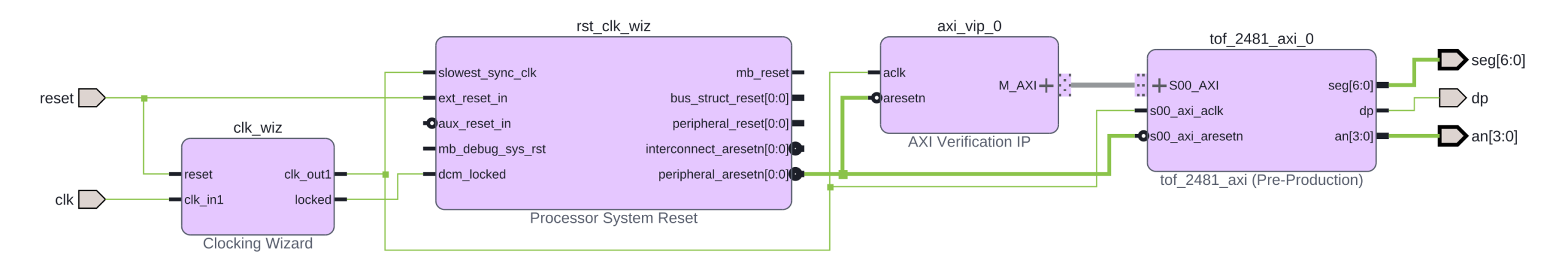
AXI Architecture for Simulation
Because simulation is distinct from synthesis, it is handy to have a separate Vivado block diagram for simulation. The reason is that we need a lot of infrastructure to generate the AXI bus signals, and this is already provided by the big players who have skin in the AXI game: AMD, ARM and the likes. It would be very difficult to toggle all AXI signals of a transaction by hand (remember that an AXI-compliant IP has tens of ports; one has to address a 32-bit address space, for example). Thankfully, this is already done by an IP block that contains only simulation code and is called “AXI Verification IP”. The resulting block diagram for the simulation is shown below.
It turns out that to connect to such a beast as an AXI-bus; it does not use the relatively basic simulation primitives of the original Verilog. One needs more abstraction, and it is provided by the dynamic extended features of System Verilog which extends the original Verilog for system verification. The code excerpt below shows the gist of the test-bench and illustrates how easy it is to generate an AXI transaction.
`timescale 1ns / 1ps

import axi_vip_pkg::*;
import design_2_axi_vip_0_0_pkg::*;

module tb_tof_2481_axi;
 WE// ⋮ (module definition and DUT instantiation)
  initial begin
      // ⋮ (code omitted)
      master = new("master", dut.design_2_i.axi_vip_0.inst.IF);
      master.start_master();
      // ⋮ (code omitted)
      master.AXI4LITE_WRITE_BURST(32'h44A0_0000,
                                  3'b000,
                                  32'h0000_BEEF,
                                  resp);
      $display("WRITE 0 resp=%0d", resp);
      master.AXI4LITE_WRITE_BURST(32'h44A0_0004,
                                  3'b000,
                                  32'h0000_FFFF,
                                  resp);
      $display("WRITE 1 resp=%0d", resp);
      // ⋮ (code omitted)
      $finish;
  end
endmodule
Having concocted the above test-bench for sending the input signals to the simulation of the AXI connected 7-segment LED display, we can click in Vivavdo, and lo-and-behold, wave-forms come out.
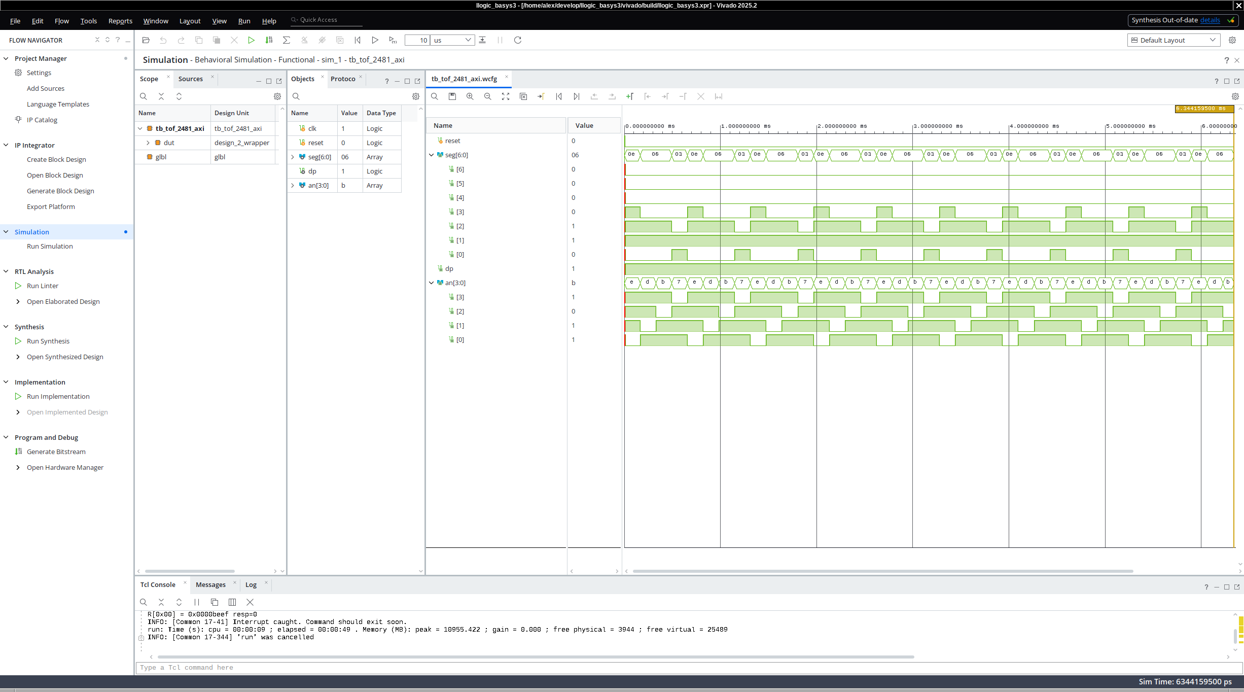
Of course, to perform even further testing and validation of the seven segment LEDs, one could convert the individual signals driving the LEDs to hexadecimals signals and could compare what the LEDs show to what the AXI master sent (in our case the hexadecimal value of 0xbeef). But the journey toward model checking, automatic diagnostics and testing is more interesting, and we have discussed LEDs more than enough.
Reflection
FPGA programming tool chains and Vivado are a hairball of design by committee, we do something this way because we did it the same way when we were young and when we used to bike ten miles to school every day (uphill both ways and into the wind). On the more positive side, these are complex tools, and they work, and people use them for their digital design.
All that being said, our understanding of both the theory and practice of computing has improved dramatically since the mid 20-th century, and it is time to revisit these old ways of designing and implementing circuits. If we do this carefully, maybe, maybe, we will design the hardware, software, and even AI algorithms that are not shameful to write about and use.
What is Next?
In what follows, we will grow our demo and I will show you how crappy the actual FPGA implementation that Vivado does. We will also discuss more accurate simulations, clocks, frequencies, timing analysis, and what proper AI algorithms (not the ones everybody is discussing but the ones that are not used for fraud and deception).
The Real Deal
Unlike what is these days practice in most of the Silicon Valley, everything I talk about is accessible and reproducible. So here is the repository that allowed me to write this blog article and make the demo:
https://gitlab.llama.gs/llogic_basys3
Ceterum censeo slopem esse delendam.
(Cato the Elder ended every speech in the Roman Senate with “Carthage must be destroyed” — regardless of the topic. This is that, but for AI slop.)